The IMS cleanroom at Georgia Tech is equipped with various lithography tools, each designed to meet different processing needs. These tools provide precise control over the shape and size of the patterns created, allowing for cost-effective patterning over entire surfaces. The equipment includes advanced systems for both traditional photomask-based lithography and direct laser writing.
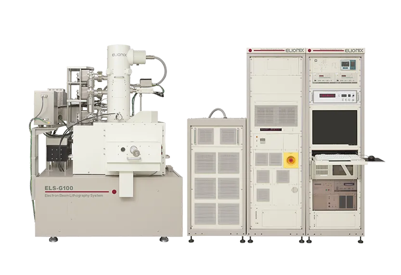
Elionix ELS-G100 Electron-Beam Lithography System
The Georgia Tech Elionix ELS G-100 is a high-speed, ultra-high-precision thermal field emission (TFE) electron beam lithography system designed for advanced nanofabrication. It achieves 6 nm line widths with a stable 1.8 nm electron beam at 100 kV, supporting commercially available resists. A high-precision laser interferometer stage ensures 15 nm stitching and 20 nm overlay accuracy. It enables uniform fine pattern writing across a 500 μm field without stitching, enhancing speed and accuracy. Accommodating substrates from small pieces to 8-inch × 8-inch samples, the ELS G-100 is ideal for high-resolution applications in nanotechnology, semiconductors, and quantum devices.
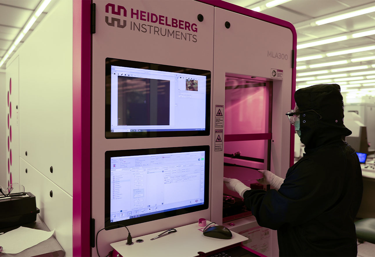
Heidelberg MLA 300
The Georgia Tech Maskless Aligner MLA 300 is engineered for high-volume production, delivering exceptional flexibility and precision in industrial lithography. Capable of accommodating wafers up to 300 x 300 mm, it dynamically adjusts to surface variations, eliminating the need for expensive and time-consuming mask fabrication. The system utilizes 375 nm and 405 nm wavelengths for exposure and features industry-standard optical and pneumatic autofocus mechanisms. With its high throughput and cutting-edge accuracy, the MLA 300 revolutionizes sample exposure in advanced manufacturing.
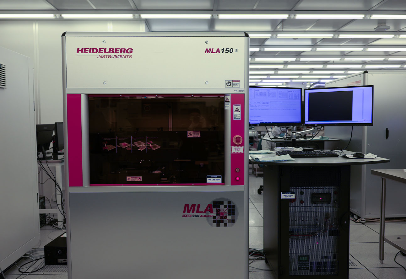
Heidelberg MLA 150 1 and 2
The Georgia Tech Maskless Aligner MLA 150 is a cutting-edge lithography tool designed for applications in quantum devices, MEMS, micro-optics, sensors, and life sciences. Eliminating the need for masks, it enables rapid design modifications and reduced cycle times. With resolutions of 0.6 µm and 1 µm, it supports 375 nm and 405 nm wavelengths for various photoresists. The system handles substrates from 0.5 cm × 0.5 cm up to 8 inches × 8 inches, accommodating diverse fabrication needs. It offers high-speed exposure—100 × 100 mm² in under 10 minutes—and sub-500 nm multi-layer alignment accuracy, ensuring unmatched precision and flexibility.
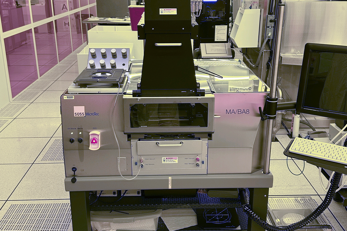
Suss MicroTec MA8/BA8 mask aligner
The Georgia Tech SUSS MA/BA8 Gen 4 mask aligner is the latest mask and bond aligner from SUSS MicroTec, designed for research, development, and small-scale production. It accommodates substrates up to 200 mm and supports photonic device fabrication for bio-photonics and quantum dot displays. Featuring ergonomic design, intuitive alignment software, and advanced data logging, it simplifies exposure setup while minimizing errors. The system integrates patented MO exposure optics, combining High Resolution (HR) and Large Gap Optics (LGO). It offers 0.7 µm resolution, multiple contact modes—including vacuum and hard contact—and backside alignment. LED light sources enhance efficiency and sustainability.
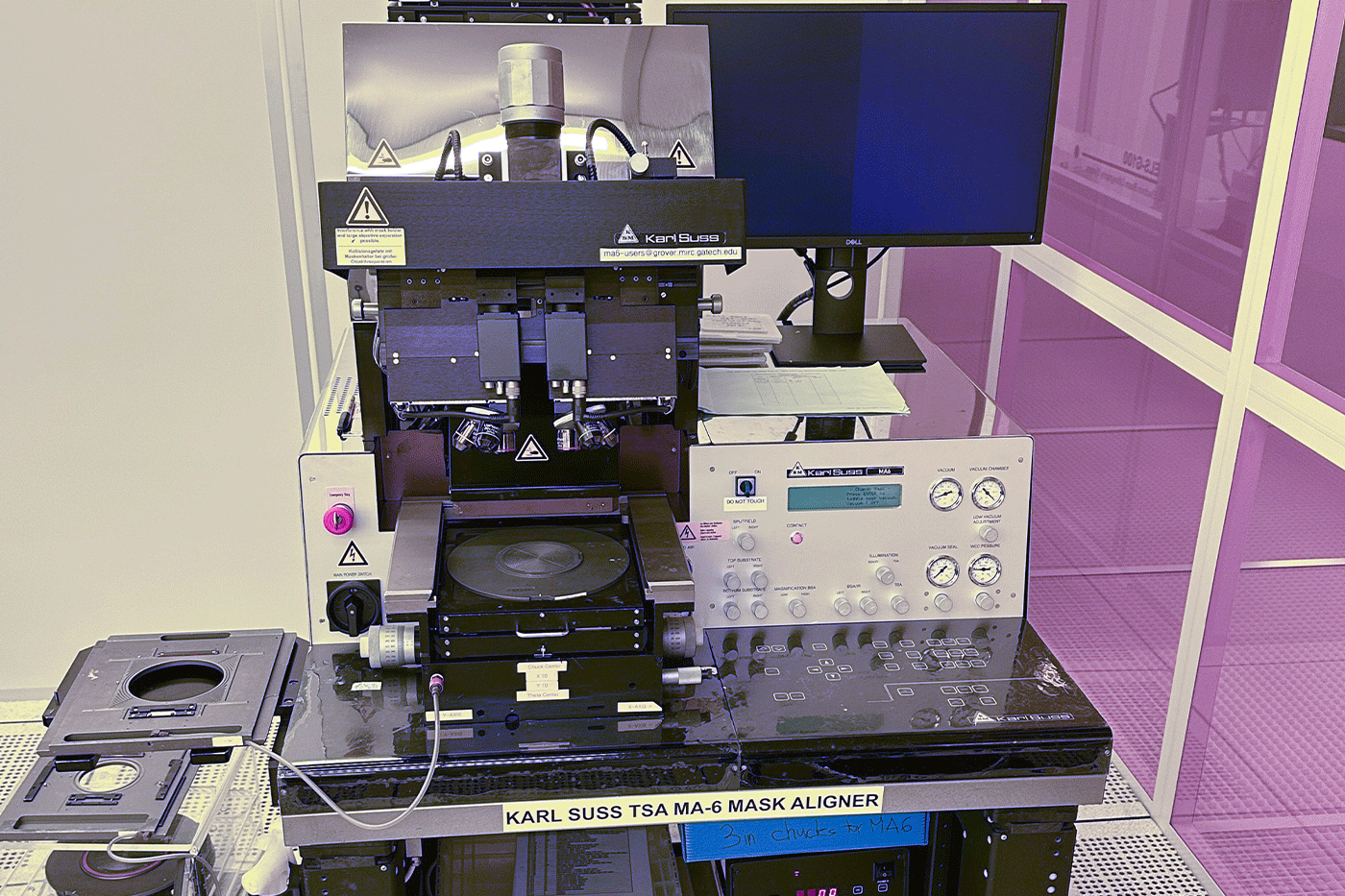
Karl Suss TSA MA-6 Mask Aligner- Marcus
Located in the Marcus Nanotechnology Building Inorganic Cleanroom, the Karl Suss TSA MA6 Mask Aligner offers high quality exposure optics for high resolution and optimum edge quality with 0.2 micron top alignment resolution. This mask aligner offers accurate and precise gap settings for high yield and contains high intensity light sources that reduce process time. It is optimized for top size alignment (TSA) and is capable of processing up to 6"/150mm wafers. The components consist of UV250 optics and monitor and Olympus 5x, 10x, and 20x objectives lenses.
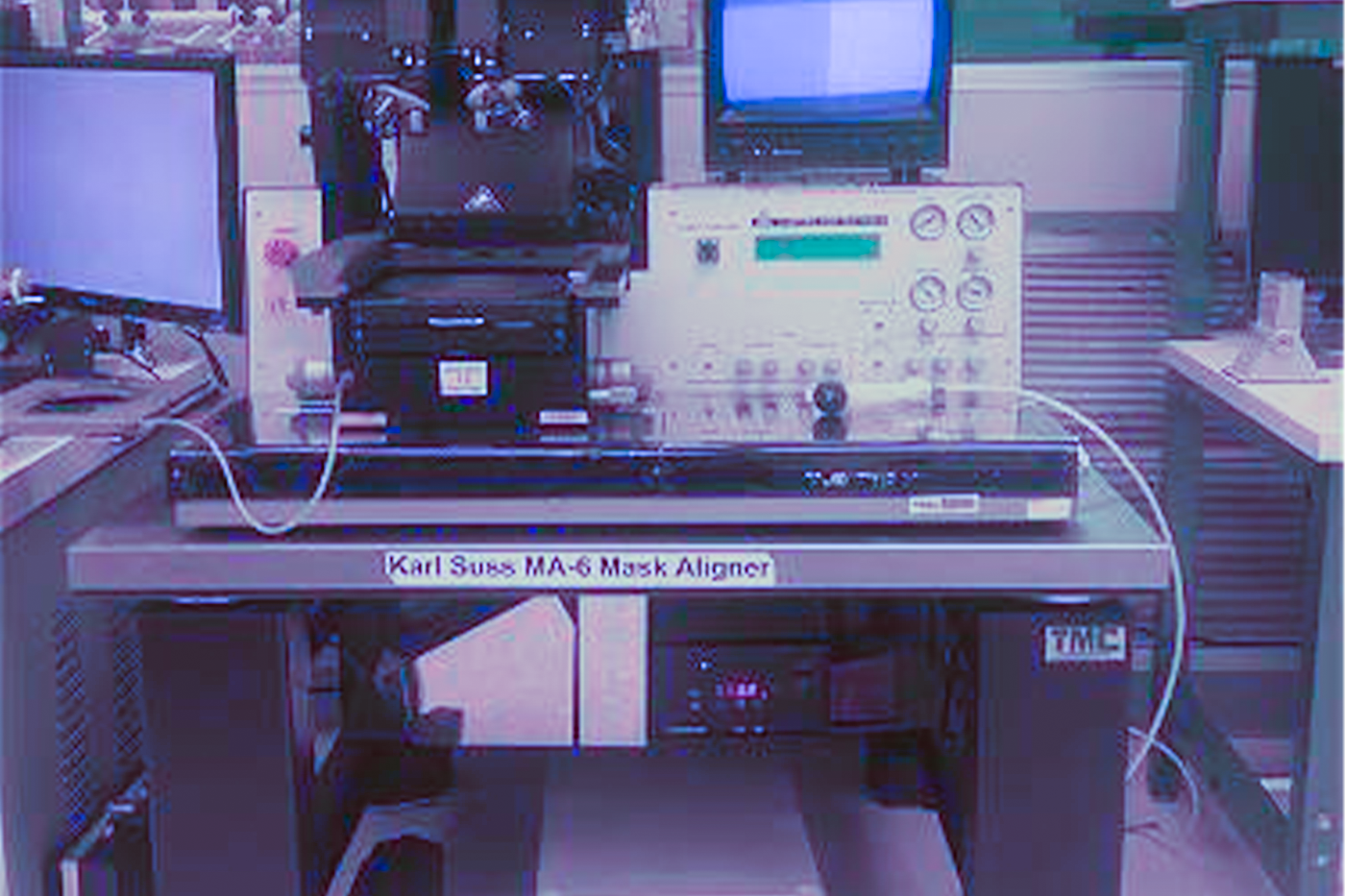
Karl SUSS MA-6 Mask Aligner - Pettit
Located in the Pettit cleanroom at Georgia Tech, these mask aligners are used in photolithographic processes to transfer a pattern from a mask to a photoresist coating on the substrate. The MA-6 can handle wafers up to 6" in size, and is optimized for 435 nm wavelength.
Spin Coaters
Osiris Spin Coater
The Osiris Spin coater is a part of the photolithography equipment group and is used for semiconductors and microelectronics applications. Osiris spin coater supports wafer sizes of 8-inch, 6-inch, and 4-inch. Users are permitted to spin up to 6000 RPM for safety and performance reasons. The Osiris spin coater supports edge bead removal up to 500 RPM, making it suitable for applications requiring precise coating control. This versatility makes the Osiris ideal for a wide range of coating applications, including research and development, and prototyping. Its ability to coat substrates, combined with EBR functionality, ensures high-quality results with minimal material waste.

Suss Microtech Labspin 6
The LabSpin6 spin coater is designed for the application of liquid coating materials onto various substrates. It features the capability to perform Edge Bead Removal (EBR), ensuring clean and uniform edges. The LabSpin6 is equipped with chucks to accommodate both small pieces and wafers up to 6 inches in diameter. It is suitable for round substrates with diameters up to 8 inches and square substrates up to 4 inches. This versatility makes LabSpin6 ideal for a wide range of coating, including small-scale production, where precision and consistency are critical. Its ability to handle both small and larger substrates, combined with EBR functionality, ensures high-quality results with minimal material waste.
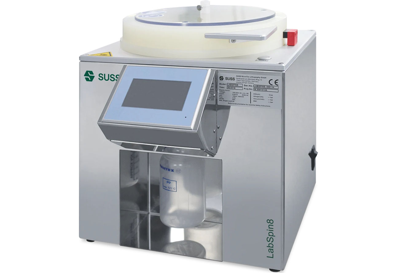
Suss Microtech Labspin 8
The LabSpin8 spin coater is designed for the application of liquid coating materials onto various substrates. It features the capability to perform Edge Bead Removal (EBR), ensuring clean and uniform edges. The LabSpin8 is equipped with chucks to accommodate both small pieces and wafers up to 8 inches in diameter. It is suitable for round substrates with diameters up to 8 inches and square substrates up to 4 inches. This versatility makes LabSpin8 ideal for a wide range of coating, including small-scale production, where precision and consistency are critical. Its ability to handle both small and larger substrates, combined with EBR functionality, ensures high-quality results with minimal material waste.
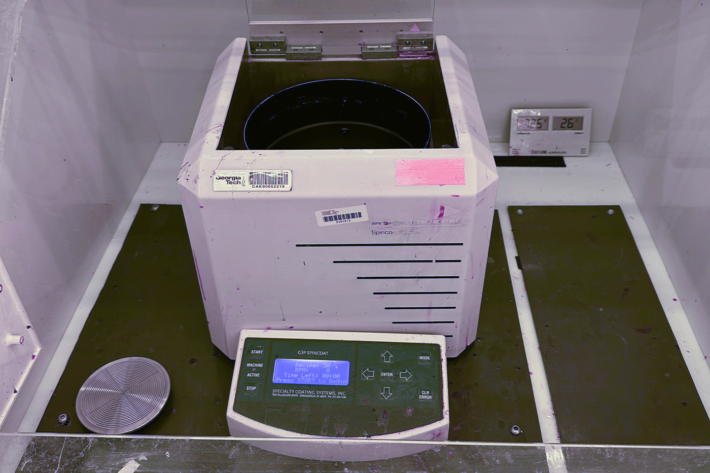
SCS G3P8 Spin Coater
The SCS G3 Spin Coater Series is a programmable tool designed for the application of liquid materials on substrates. It offers process control, making it suitable for thin-film deposition applications. The SCS G3 can store and execute up to 30 unique programs, each consisting of up to 20 customizable steps. Spin speeds are adjustable from 0 to 5,000 RPM, with ramp times ranging from 0.1 to 25.5 seconds. Designed to accommodate a variety of substrate sizes, the spin coater is equipped with specialized chucks for wafers or pieces ranging from 1-4 inches in diameter. This capability makes it ideal for both small-scale and research-oriented projects as well.
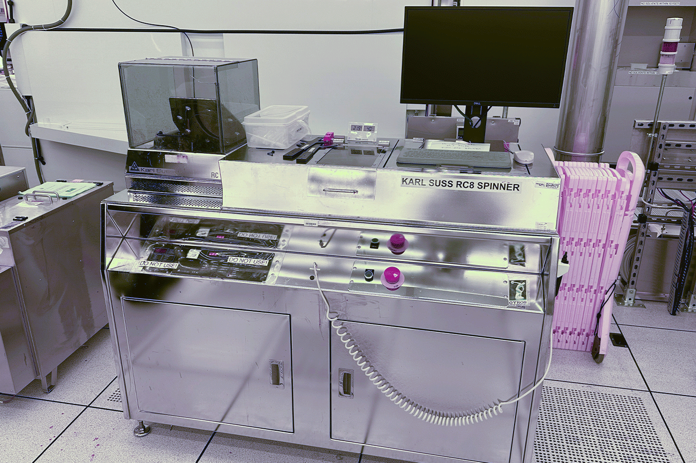
Karl Suss RC8 Spinner
The Karl Suss RC8 programmable process spinner is a tool specifically designated for photoresist coating applications. The RC8 is strictly reserved for photoresist use while spin coating of other materials must be conducted using alternative spinners available in the facility. The RC8 offers precise and programmable control over coating parameters, with a maximum spin speed of 5,000 rpm and an adjustable acceleration rate ranging from 100 to 1,000 rpm/s. Its ability to produce highly uniform coatings on varying substrate types ensures consistent and reliable results in demanding microfabrication environments.
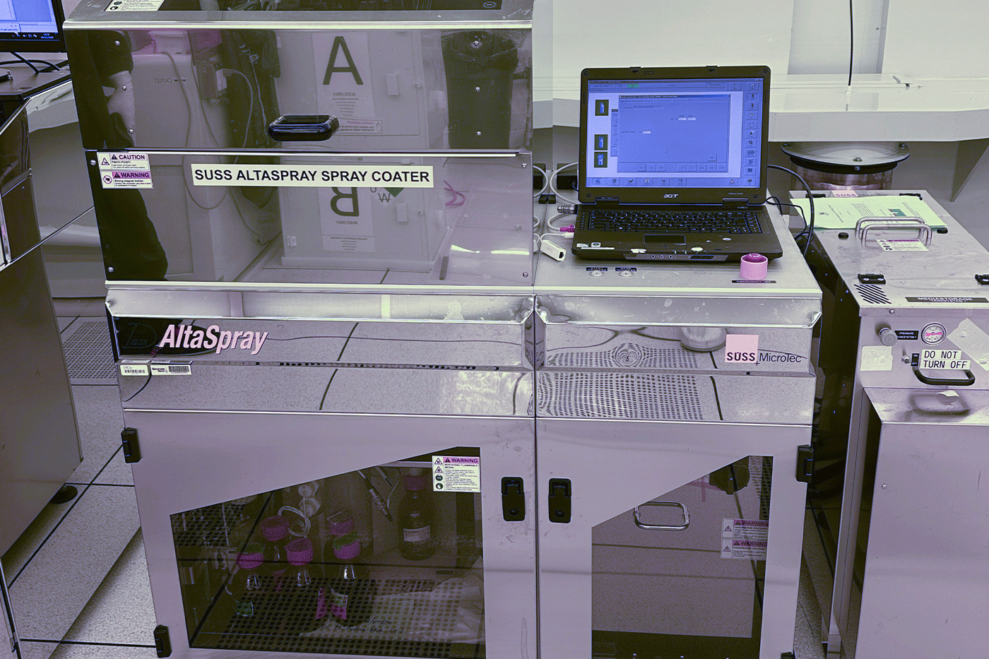
Suss Alta Spray Coater #1
SUSS MicroTec’s proprietary AltaSpray coating technology is a unique resist deposition method that is capable of producing highly uniform resist films on different 3-D microstructures. The AltaSpray technology is capable of coating 90° corners, KOH etched cavities, Through Silicon Vias (TSVs) or lenses with topographies ranging from a few microns to 600µm or more. The ability to produce conformal resist coatings on severe topography makes them the ideal choice for R&D, MEMS, 3D-Integration and Wafer Level Packaging applications like 3D image sensor packaging. The tool handles wafer up to 8 in. Chuck temperature is set at 60C. The available resists are: AZ P4620, SC1827, and NR7-3000p.

Suss AltaSpray Spray Coater #2
SUSS MicroTec’s proprietary AltaSpray coating technology is a unique resist deposition method that is capable of producing highly uniform resist films on different 3-D microstructures. The AltaSpray technology is capable of coating 90° corners, KOH etched cavities, Through Silicon Vias (TSVs) or lenses with topographies ranging from a few microns to 600µm or more. The ability to produce conformal resist coatings on severe topography makes them the ideal choice for R&D, MEMS, 3D-Integration and Wafer Level Packaging applications like 3D image sensor packaging. The tool handles wafer up to 4 in. Chuck temperature is set at 60C. The available resists are AZ P4620, SC1827, and NR7-3000p.
Suss Microtec ACS200
The Suss MicroTec ACS200 is an automated photoresist coating and baking station with cassette-to-cassette substrate operation. It supports spin coating of photoresist on a variety of substrates. The tool provides complete resist coating capabilities, including hotplate baking up to 250 °C and automated edge-bead removal with backside rinse. The tool handles 4 in and 6 in full wafers, equipped with HDMS oven, 2 hotplates, 1 cool plate, 1 coating module and 1 developing module. It supports 3 resists: S1813, SPR220-7.0 and NR9-1500py, 2 developers: MF-319 and RD-6.