Lithography
IMS offers advanced lithography tools for micro- and nanofabrication, including Elionix ELS-G100 e-beam, Heidelberg MLA maskless aligners, and SUSS MA6/MA8 mask aligners. These systems enable high-resolution patterning for semiconductors, MEMS, photonics, and quantum devices.
Etching
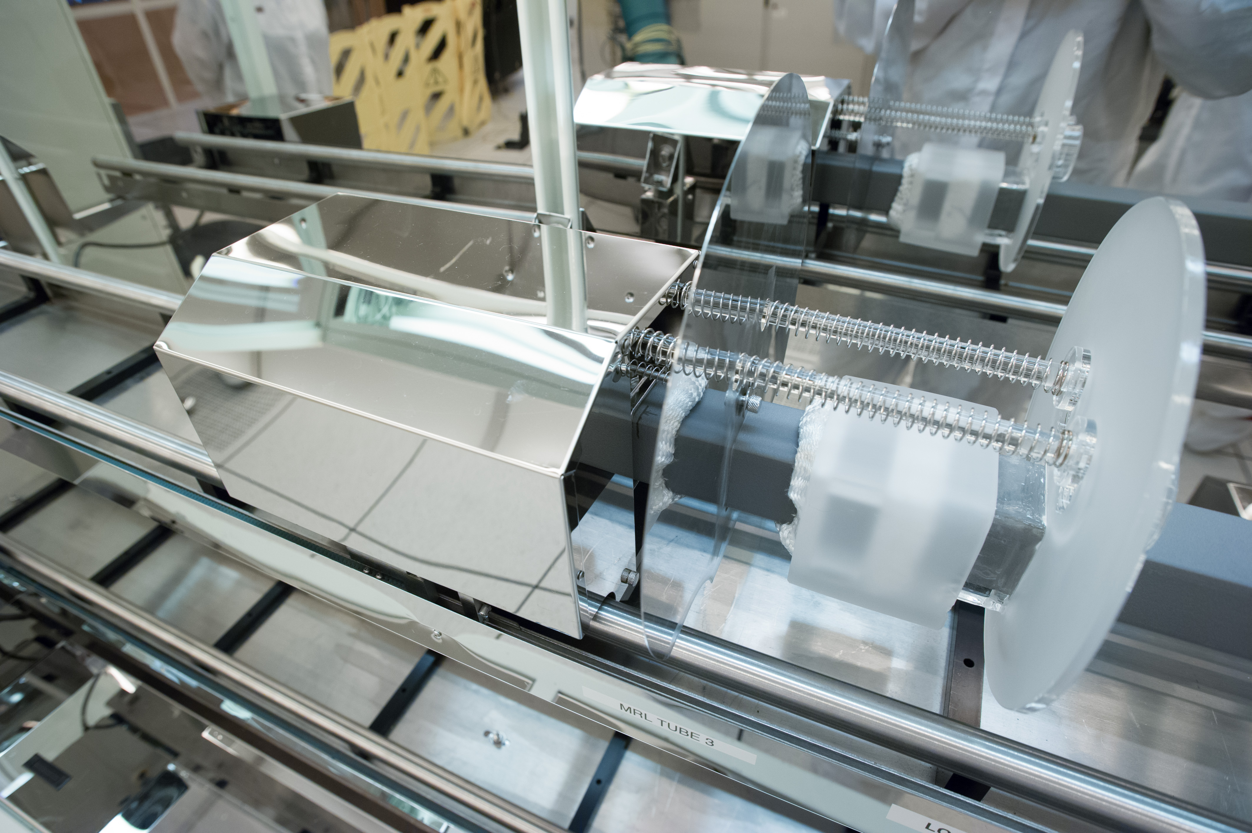
IMS cleanroom offers advanced etching capabilities, including DRIE/Bosch, ICP, RIE, and XeF₂. With tools like KLA SPTS Rapier, STS Pegasus, Plasma-Therm Versaline, and Xactix XeF₂, we enable high-aspect ratio silicon etching, dielectric patterning, and isotropic release for MEMS, photonics, and packaging.
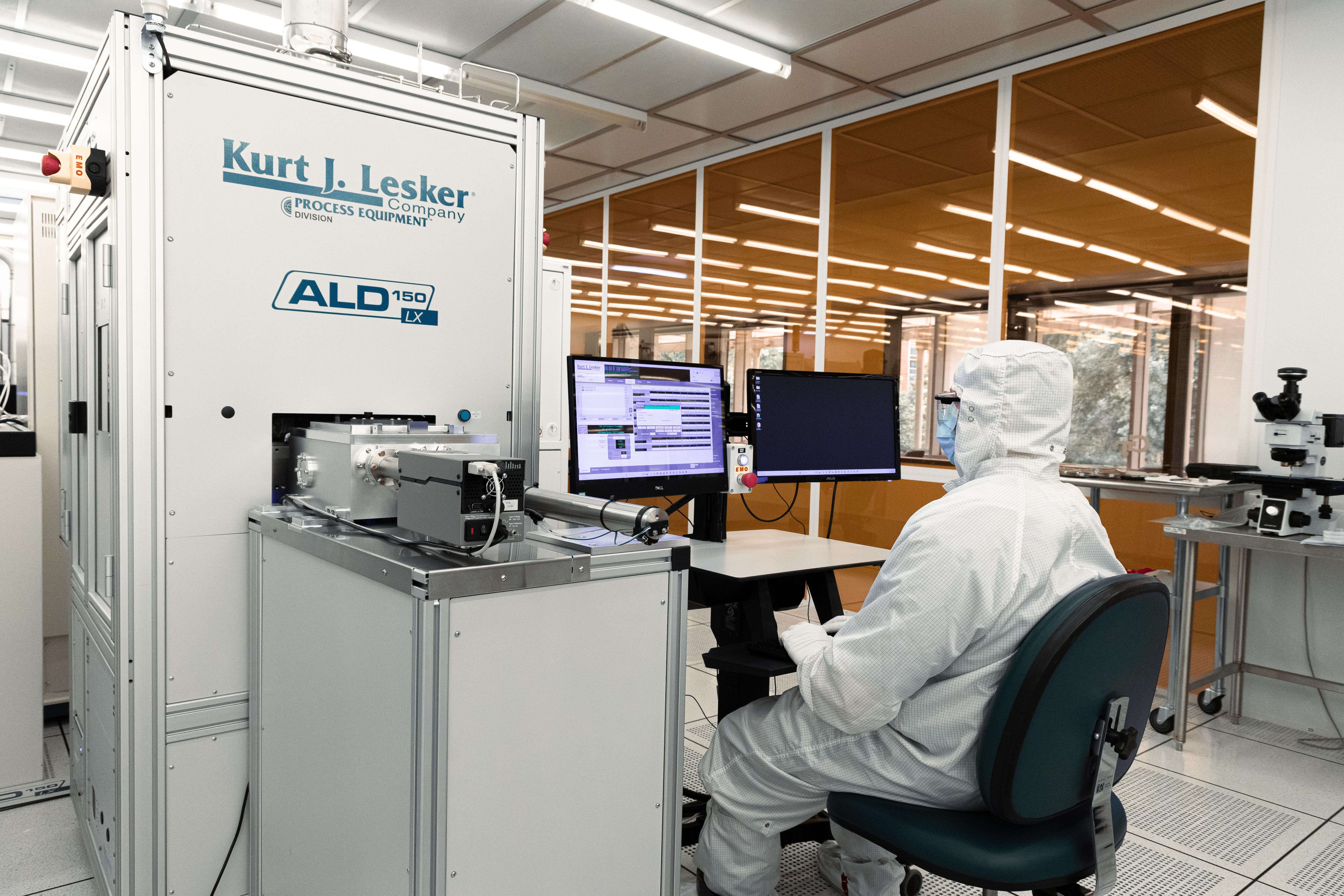
Atomic Layer Deposition
IMS cleanroom features advanced ALD systems—Cambridge Fiji, Veeco Fiji G2, Kurt J. Lesker ALD150LX, and Oxford FlexAL—offering thermal and plasma-enhanced deposition. These tools deliver precise, conformal films of oxides, nitrides, and metals on substrates up to 200 mm at temperatures to 600°C.
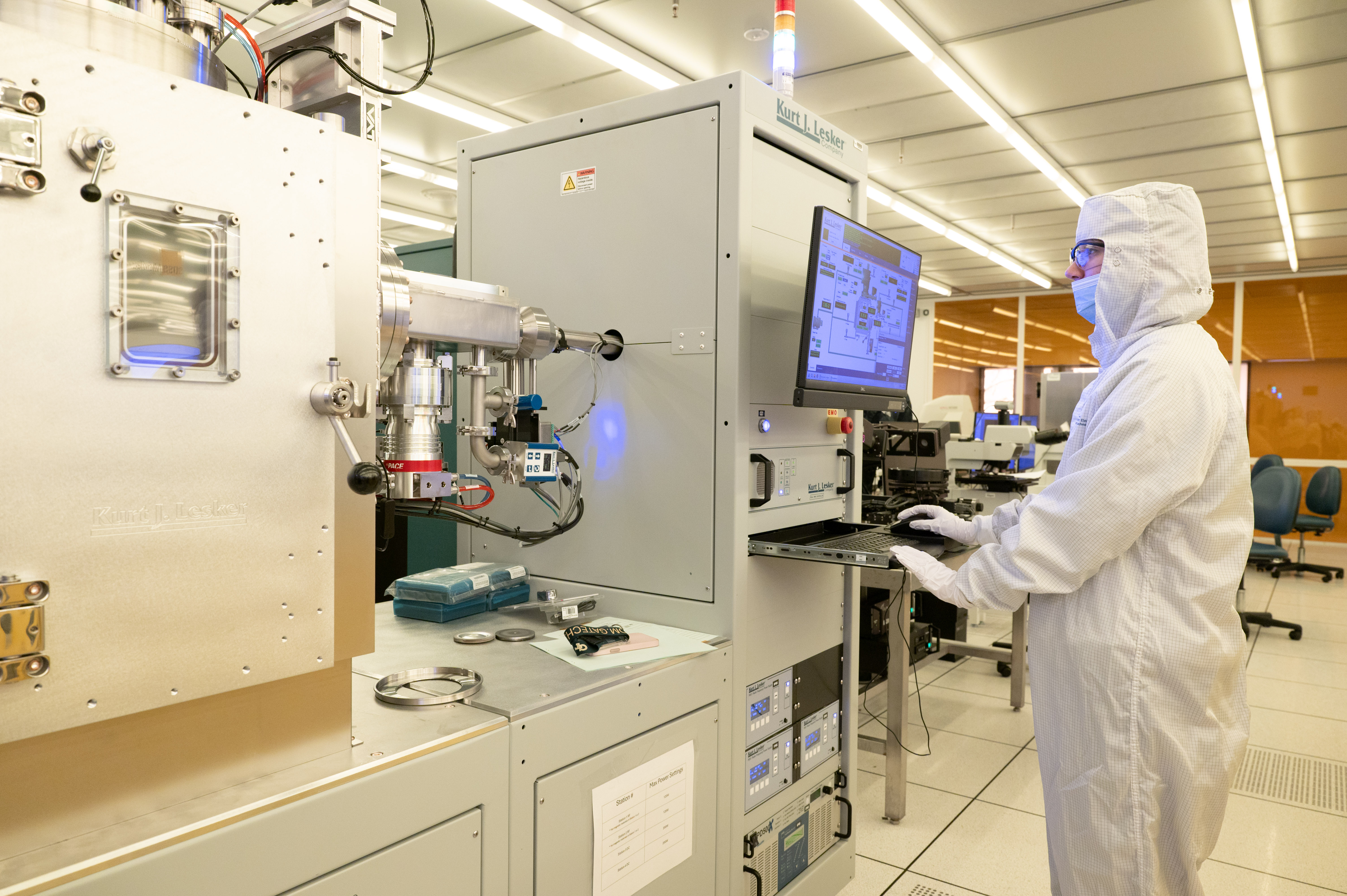
Physical Vapor Deposition
IMS PVD capabilities include e-beam and filament evaporators plus RF/DC sputtering systems for precise thin-film deposition of metals, dielectrics, nitrides, and chalcogenides. Supporting co-deposition and multi-source sputtering, IMS delivers uniform films for microelectronics, photonics, and advanced materials.
Chemical Vapor Deposition
IMS CVD tools enable thin-film deposition of oxides, nitrides, a-Si, poly-Si, graphene, and nanowires. Systems include PECVD, HDPCVD, LPCVD, APCVD, and thermal CVD. Oxford ICP-PECVD and Plasma-Therm HDPCVD deliver high-density films, while FirstNano and Black Magic support graphene, nanowire, and CNT growth.
Thermal Furnaces
IMS Furnace Suite supports oxidation, diffusion, annealing, LPCVD, sulfurization, graphene growth, and nanowire synthesis. With vacuum ovens, RTP, and high-temp CVD furnaces, users achieve precise thin-film growth, doping, and thermal treatments for semiconductor and nanomaterial research.
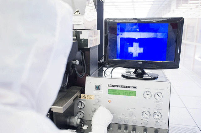
Metrology
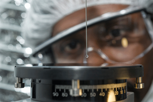
IMS Cleanrooms offer advanced metrology tools for thin films, wafers, and nanostructures. Capabilities include thickness measurement, surface profiling, stress analysis, and imaging with tools like Hitachi FE-SEM with EDS, profilometers, ellipsometry, and sheet resistance measurement.
Wet Processing
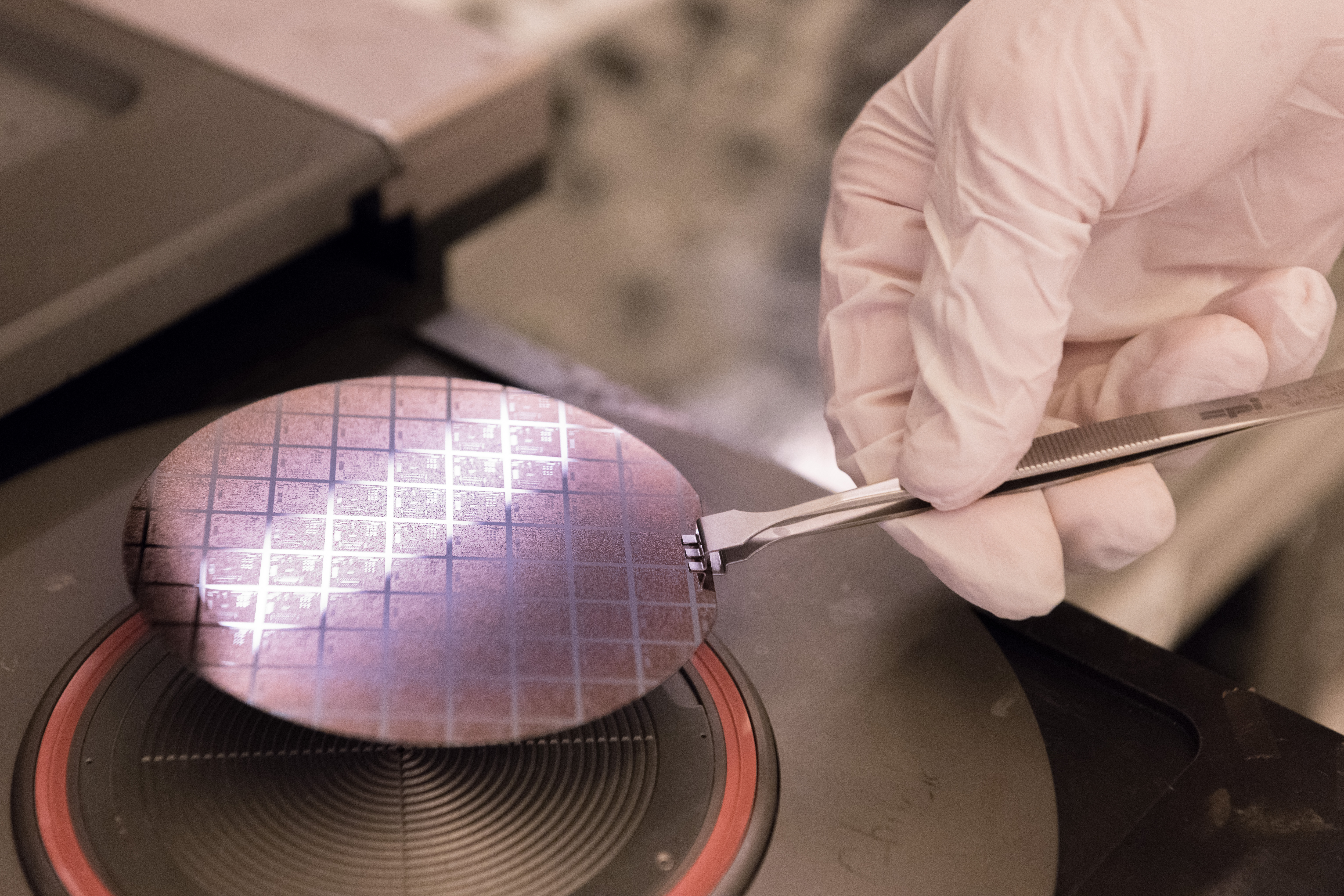
IMS Cleanroom wet processing area offers chemical stations for wafer cleaning, etching, electroplating, and solvent handling. Capabilities include CMOS-qualified benches, solvent and acid/base hoods, multi-metal plating for Ni, Cu, Au, and PV clean benches—supporting high-purity microfabrication.