The IMS cleanroom at Georgia Tech offers a comprehensive suite of metrology capabilities essential for micro/nano fabrication. These include advanced imaging tools like scanning electron microscopes (SEMs) and profilometers for surface characterization, ellipsometers for thin film analysis, and various spectrometers for material composition analysis. The facility also features stress measurement tools and four-point probes for electrical characterization, ensuring precise and accurate measurements for research and development.
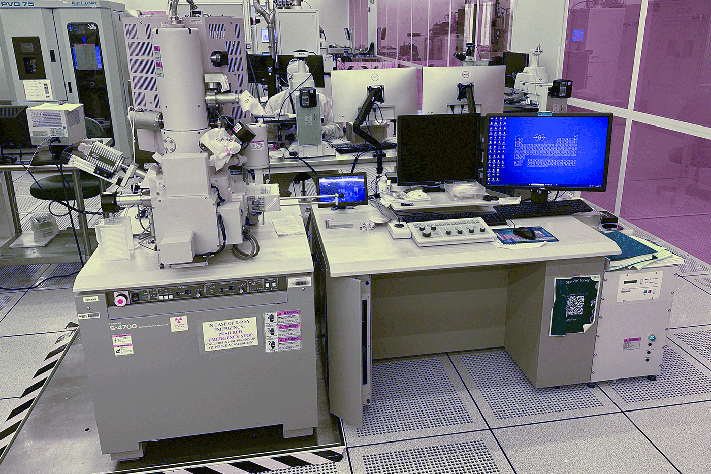
Hitachi S-4700 FE-SEM
The Hitachi S-4700 FE-SEM at Georgia Tech is a high-performance cold field emission scanning electron microscope designed for ultra-high resolution imaging of micro- and nanoscale materials. Ideal for the analysis of thin films, semiconductor devices, and nanostructures, this system provides exceptional surface detail and edge resolution, particularly on exceptionally clean and well-prepared specimens.
Operating at accelerating voltages from 0.5 to 30 kV, the S-4700 achieves a secondary electron resolution of 1.5 nm at 15 kV, enabling high-quality imaging at both high and low voltages. The microscope supports both secondary and backscattered electron imaging modes, offering flexibility in visualizing topography, morphology, and material contrast.
The system is equipped with an integrated Bruker EDAX Energy Dispersive X-ray Spectroscopy (EDS) detector, allowing users to perform elemental analysis and compositional mapping directly within the SEM chamber. This combination of imaging and analytical capabilities makes the S-4700 an essential tool for researchers in materials science, nanotechnology, microelectronics, and related fields.
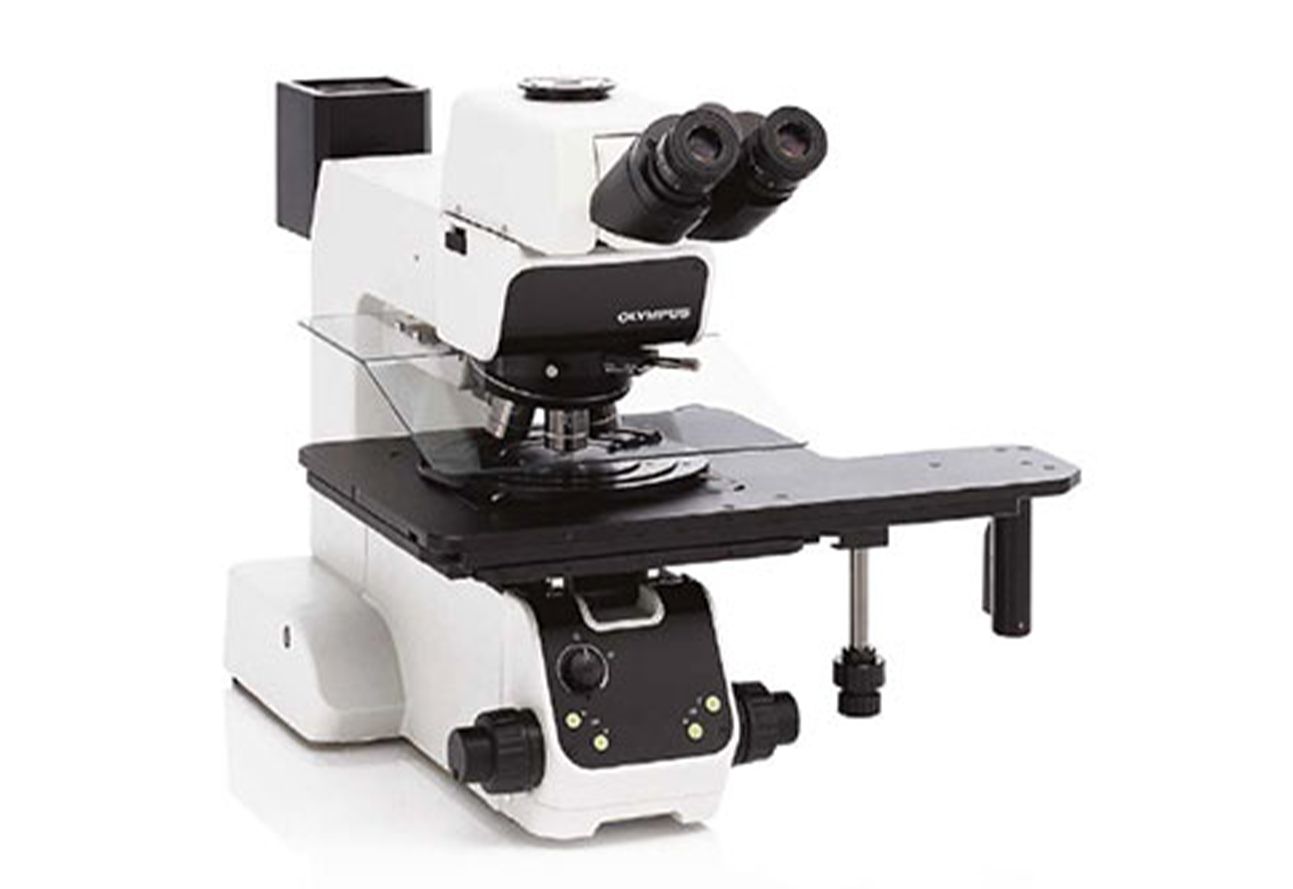
Olympus MX61 M1&M2
The Olympus MX61 Microscope delivers image resolution and clarity, enhanced by the imaging software for precise and high-quality image capture. It supports multiple viewing modes, including brightfield, darkfield, and optical path settings, allowing for optimal exposure and detailed visualization of substrates. With a range of objective lenses (5x, 10x, 20x, 50x, and 100x), the MX61 suits different analysis needs. The stage features both coarse and fine adjustment through a clutch handle, enabling smooth and precise sample positioning. Advanced capabilities include image acquisition, specialized image processing, measurement functions, and statistical analysis. These features make the MX61 an ideal tool for material inspection, defect analysis, and research applications.
Microscope M1 (Olympus MX61) | (IMS) IMS- Micro/Nano Fabrication Facility
Microscope M2 (Olympus MX61) | (IMS) IMS- Micro/Nano Fabrication Facility
Olympus MX61 Microscope | (IMS) IMS- Micro/Nano Fabrication Facility
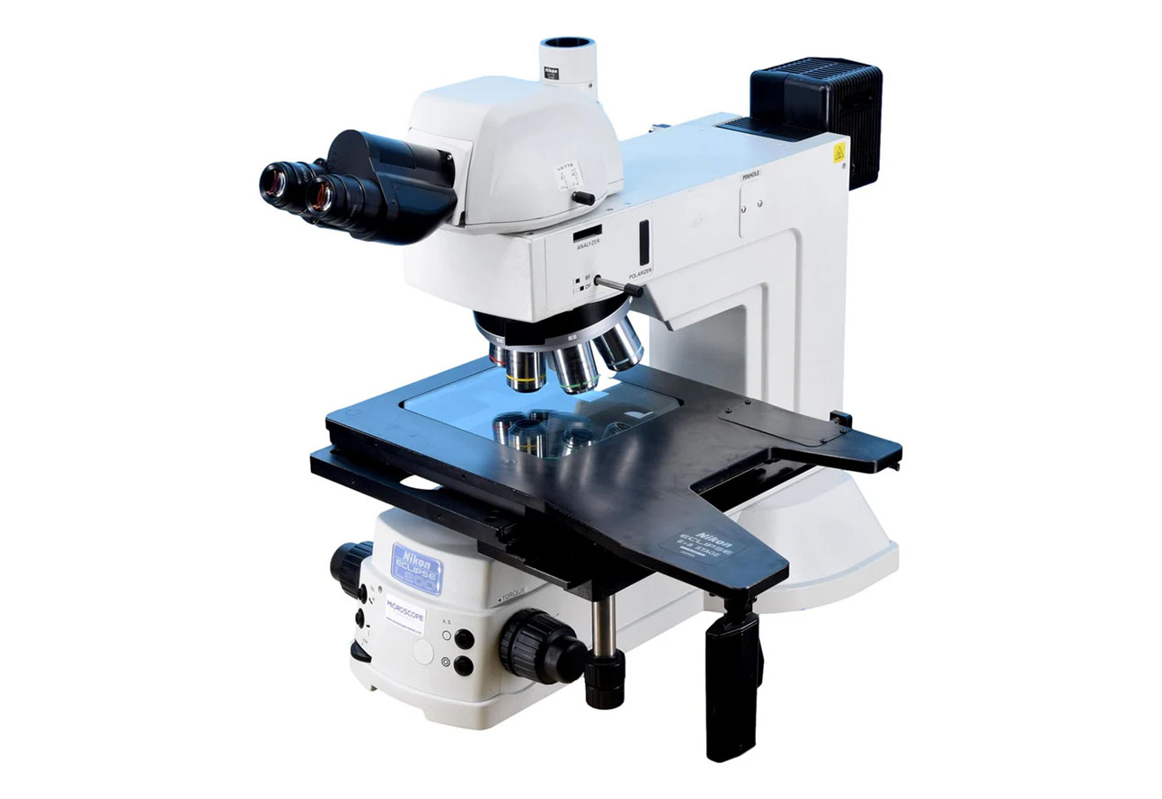
Nikon L200 M4 & M5
The Nikon L200 Microscope delivers image resolution and clarity, enhanced by the imaging software for precise and high-quality image capture. It supports multiple viewing modes, including brightfield and darkfield, allowing for optimal exposure and detailed visualization of substrates. With a range of objective lenses (2.5x, 10x, 20x, 50x, and 100x), the Nikon suits different analysis needs. The stage features both coarse and fine adjustment through a clutch handle, enabling smooth and precise sample positioning. Advanced capabilities include image acquisition, specialized image processing, measurement functions, and statistical analysis. These features make the Nikon an ideal tool for material inspection, defect analysis, and research applications.
Microscope M5 (Nikon L200) | (IMS) IMS- Micro/Nano Fabrication Facility
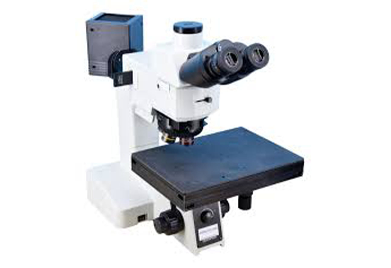
IR Microscope 4
The Olympus MX51-F IR microscope is a specialized optical instrument designed to capture and analyze materials using infrared (IR) light. The IR Microscope 4 includes various magnification options such as 10x, 20x, 50x, and 100x. By combining imaging and infrared spectroscopy, these microscopes can generate structural maps of a sample, making them valuable for identifying material defects and analyzing thin films. The Olympus Microscope is used for alignment, identification of substrate contamination and critical dimension inspections.
Nanospec Reflectometer - Inorganic
The NanoSpec 3000 is a film thickness measurement system that utilizes a modern small spot spectroscopic reflectometer that is built on a simple-to-use tabletop platform. The Nanospec 3000 is a precise AFT (Automated Film Thickness) measurement system that measures the thickness of films deposited on various substrates and its reflectance relative to silicon. Optical objective lens include 50x and 100x. It measures vertical features from 100 Å up to 0.02 mm with a resolution of 50 Å in a short 3 seconds.
Nanospec Reflectometer - Inorganic | (IMS) IMS- Micro/Nano Fabricatio
Nanospec Reflectometer - Pettit | (IMS) IMS- Micro/Nano Fabrication

Woollam M2000 Ellipsometer
The Woollam M2000 Ellipsometer is a versatile noncontact optical metrology tool, which can measure the optical reflective index and film thickness deposited on a substrate. It can measure the transparent films (0-6000 nm), semi-transparent, and even thin metal film. Film distribution and uniformity can be mapped out up to 8” wafers. Typical measurements include oxides and nitrides, photoresist, polysilicon, SOI, etc.

Dektak 150 Profilometer
The Dektak 150 is a surface profilometer (by stylus contact) capable of down to 4 angstrom step height measurement. Since the stylus is in contact with the sample surface, it is important that the profilometer only be used to measure relatively rigid films. The stylus on the profilometer scans across the sample surface in the y-direction. As it moves across the surface, the stylus moves up and down tracking surface features. This vertical displacement is recorded by the tool for measurement purposes.
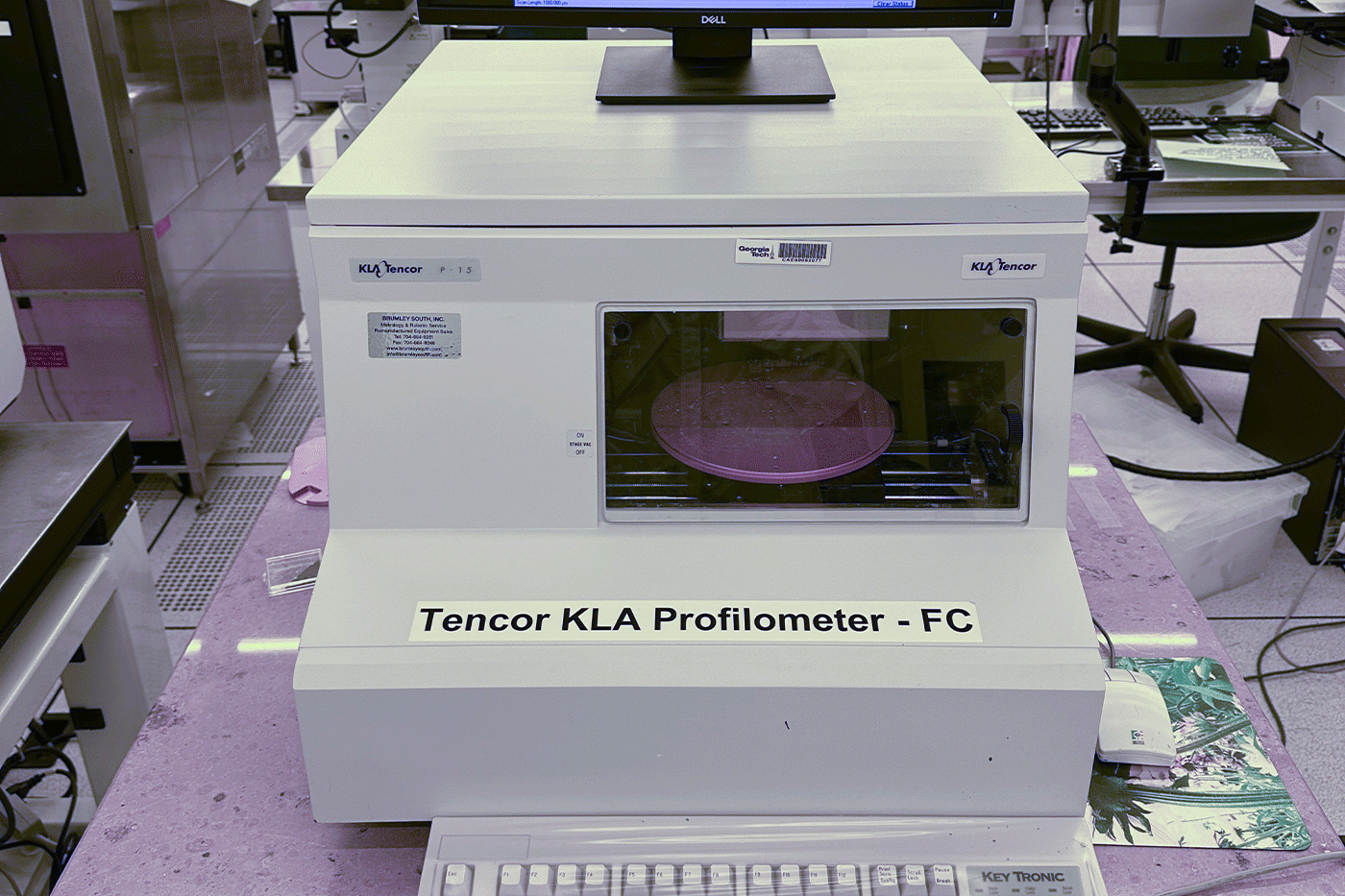
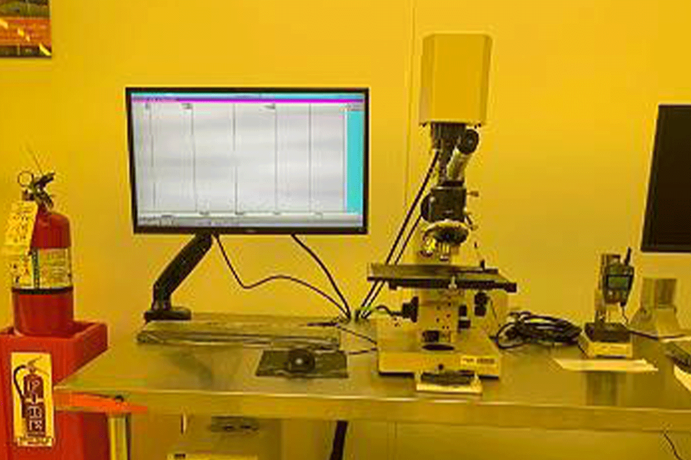
Tencor KLA P-15 Profilometer
The KLA-Tencor P-15 profiler is a highly sensitive surface profiler that measures step height and stress on a wafer surface. It can measure step height up to 130 µm for 6-inch wafer samples or smaller. It also has capabilities of measuring film stress.
Tencor KLA Profilometer | (IMS) IMS- Micro/Nano Fabrication Facility
Tencor KLA Profilometer - FC | (IMS) IMS- Micro/Nano Fabrication Faci
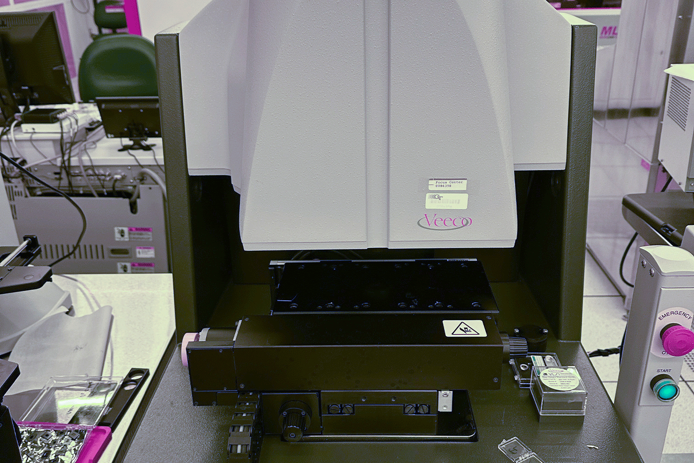
Wyko Profilometer NT 3300
The noncontact profilometer Wyko NT 3300 uses the phase change of light reflecting from various heights of similar materials to measure the uniformity of a flat surface or the horizontal distance between two adjacent surfaces. It has features includes motorized objectives and stages and an upgraded Veeco “Vision” software with additional features.
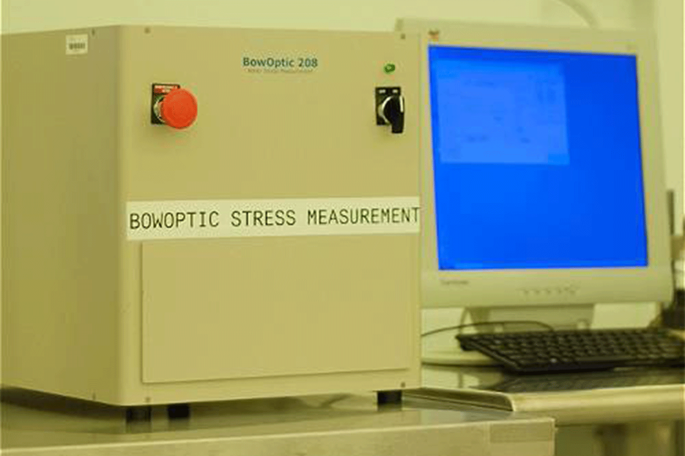
Bowoptic Stress Measurement
The BowOptic 208 at Georgia Tech is a fully automated wafer stress measurement system designed for precise, non-destructive evaluation of mechanical stress in thin films and substrates. Utilizing a highly accurate optical method based on laser beam deflection, this system measures wafer bow and curvature to determine intrinsic stress with excellent repeatability and sensitivity. Capable of handling wafers up to 8 inches in diameter, the BowOptic 208 features an automated loading mechanism that ensures consistent alignment and reliable measurements across the wafer surface. The tool is optimized for use with a wide range of materials and thin film types, making it ideal for applications in semiconductor process development, MEMS fabrication, and advanced material research. With user-friendly software, real-time data analysis, and high-throughput capabilities, the BowOptic 208 provides critical feedback for process optimization, layer uniformity evaluation, and quality control in both research and industrial environments.

Signatone Four-point Probe
The Signatone Four Point Probe measures sheet resistivity on both blank wafers and wafers with a thin layer. The probe measures resistivity less than 1 ohm.